In the high-stakes world of high-performance computing, we are currently facing a brutal asymmetry. While GPU processing power (FLOPS) has been skyrocketing, the “fuel line”—our memory bandwidth—has struggled to keep up. This phenomenon, known as the “Memory Wall,” is the primary bottleneck preventing Large Language Models (LLMs) from reaching their true potential.
As someone obsessed with “tuning” systems for peak performance, I see NVIDIA’s roadmap not just as a hardware update, but as a structural revolution. Let’s break down how the Vera Rubin and upcoming Feynman architectures are rewriting the laws of semiconductor physics to kill this bottleneck once and for all.
1. The Vera Rubin Platform: Data Center as a Single Unit
NVIDIA is moving away from selling “parts” to selling “ecosystems.” The Vera Rubin platform is built on Extreme Co-Design, where the CPU, GPU, and networking act as a single, organic machine.
The Vera CPU and Olympus Cores
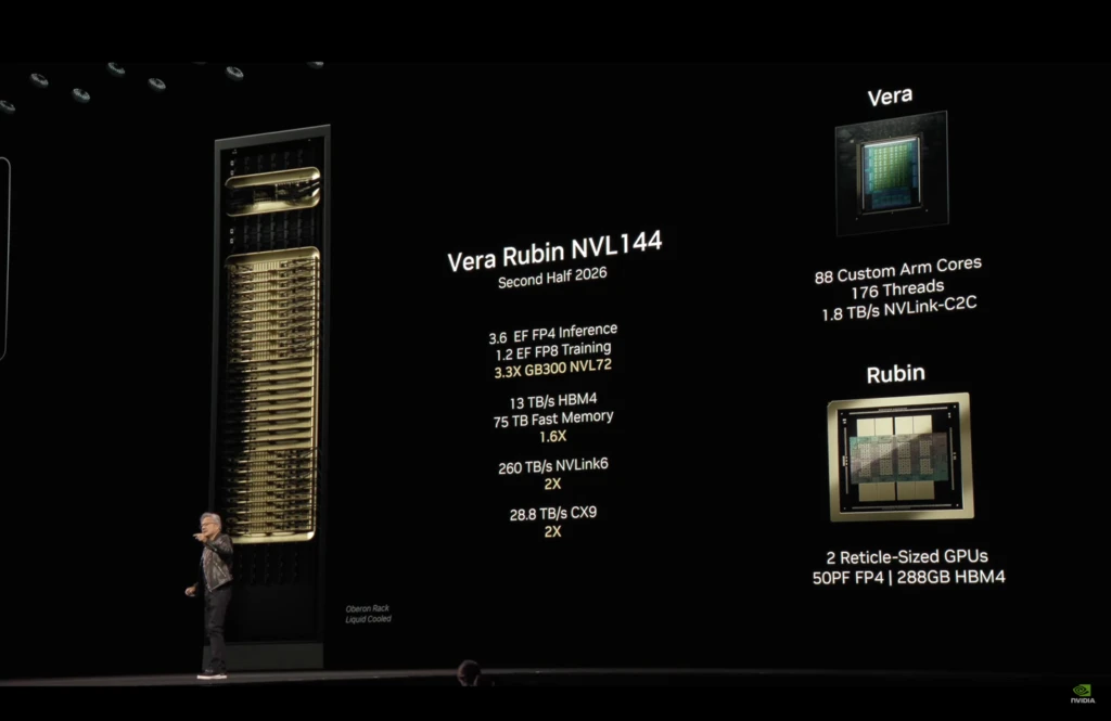
The new Vera CPU features 88 custom Olympus cores. Unlike traditional CPUs that often bottleneck the data flow to the GPU, Vera utilizes Spatial Multithreading (176 threads) to mask memory latency. With a 1.2 TB/s memory bandwidth, it ensures the GPU is never “starved” for data, making it the perfect heart for Agentic AI—where AI models perform complex, multi-step reasoning tasks.
Rubin GPU: The 3nm Beast
The Rubin GPU, manufactured on TSMC’s 3nm (N3P) process, introduces the 3rd Generation Transformer Engine. In FP4 precision, it hits a staggering 50 PFLOPS of inference performance—that is 5x faster than the Blackwell architecture.
2. HBM4: The 2048-Bit Memory Revolution
The most critical component of the Rubin architecture is HBM4 (High Bandwidth Memory 4). To solve the “Parameter Problem,” the industry has moved from a 1024-bit to a 2048-bit interface.
Efficiency and Physical Constraints
- Power Play: HBM4 reduces energy consumption per bit by approximately 40% compared to HBM3e. This efficiency is vital when a single rack (NVL72) pulls over 180kW of power.
- The Routing War: Doubling the bus width creates a massive “Crosstalk” (signal interference) risk. NVIDIA has secured 70% of TSMC’s CoWoS-L capacity just to ensure they can physically route these microscopic traces without melting the silicon.
3. Solving the MoE Bottleneck: Hybrid-EP and NVLink 6
Modern models like DeepSeek-V3 use Mixture-of-Experts (MoE), where only specific “expert” sub-networks are activated. This creates a “communication storm” as data bounces between different GPUs.
6th Gen NVLink & Hybrid-EP
NVIDIA solves this with 6.0 TB/s NVLink bandwidth and the Hybrid-EP (Hybrid Expert Parallel) software library. Hybrid-EP allows for “Computation-Communication Overlap,” meaning the GPU keeps calculating while the network card handles the data transfer in the background. This results in a 514% throughput improvement for complex MoE models.
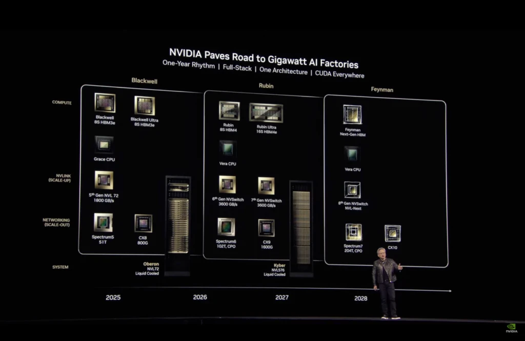
4. 2028 and Beyond: The Feynman Architecture
If Rubin is a leap, Feynman is a teleportation. Planned for 2028, it will utilize TSMC’s A16 (1nm-class) node.
Super Power Rail (Backside Power Delivery)
Traditional chips have power and signal lines tangled on the front. Feynman moves the power delivery to the back of the silicon.
- The Result: This clears up space for True 3D Stacking, where memory is placed directly on top of the logic gates. This reduces data travel distance to nearly zero, effectively “demolishing” the Memory Wall.
- 4-Bit Arithmetic: Feynman will optimize for 4-bit precision, aiming to slash AI inference costs by 10x, finally making trillion-parameter models affordable for small businesses.
Technical Specs at a Glance
| Feature | NVIDIA Blackwell | NVIDIA Vera Rubin | NVIDIA Feynman (2028) |
| Manufacturing Node | 4nm (TSMC N4P) | 3nm (TSMC N3P) | 1.6nm (TSMC A16) |
| Memory Standard | HBM3e (1024-bit) | HBM4 (2048-bit) | 3D-Stacked HBM4/5 |
| Peak Bandwidth | 8 TB/s | 22 TB/s | 40+ TB/s (Target) |
| Inference (FP4) | 10 PFLOPS | 50 PFLOPS | 200+ PFLOPS |
| Power Delivery | Front-side | Front-side | Super Power Rail (Backside) |
Conclusion: The Era of Scalable Intelligence
The transition from Blackwell to Rubin, and eventually Feynman, proves that we can no longer rely on simple transistor scaling. To win the AI race, one must master the orchestration of silicon, optics (Silicon Photonics), and software. We are no longer just building computers; we are building “AI Factories” where the bottleneck is no longer the hardware, but our own imagination.
References & Technical Sources
- NVIDIA Investor Relations: NVIDIA Kicks Off the Next Generation of AI With Rubin (2026).
- TrendForce Analysis: The Memory Wall Bottleneck and the HBM4 Supercycle.
- TSMC Technical Roadmap: A16 Process and Super Power Rail (Backside Power Delivery) Specifications.
- ArXiv [2403.14123]: AI and the Memory Wall: Historical Scaling and Future Strategies.
- SemiAnalysis Report: NVIDIA Rubin, HBM4 Yield Challenges, and the 2048-bit Interface.
- NVIDIA Developer Blog: Inside the Hybrid-EP: Overlapping Computation and Communication in MoE Models.